|
|
This site
is mobile
responsive
As a world leader in wafer level packaging technologies (WLP) and advanced packaging equipment manufacturing, PacTech has over 25 years of experience in semiconductor and electronic manufacturing industry. With our leading-edge technologies, PacTech has been a reliable partner to many global players including IDMs, OEMs and fabless design houses around the world.
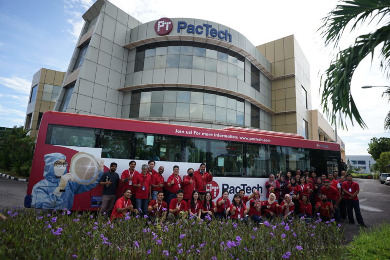
Since the establishment in Germany in year 1995 as a spin-off from the federal scientific Fraunhofer-IZM, PacTech has been expanding its footprint in the international arena by setting up PacTech USA in 2001, and searching further for a suitable location in Asia. In year 2008, with the attractive package and support from MIDA and the Malaysian government, PacTech has settled down in Bayan Lepas, Penang, to operate as our regional hub to support the Asian customers.
This year PacTech Asia is celebrating our 15 years anniversary and taking a lookback into the journey in setting up our Asian facility in Malaysia. It has been a fruitful journey despite the initial challenges in setting up the site. As PacTech came to Malaysia under pioneer status, the availability of local talent from similar technical field was scarce, however, there are abundant of Malaysians with good education level and multi-lingual background, where PacTech has managed to build up our local team to cover site operation. As of today, we have nearly 200 employees in PacTech Asia, with 98% of them are Malaysians which consists offsite directors, and over 50% of the employees have been awarded the long-service award.

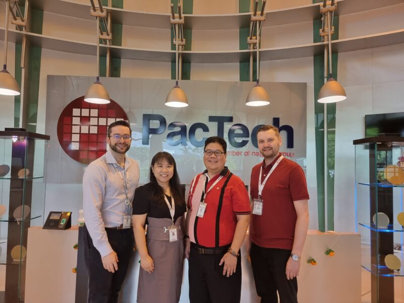
Dr. Thorsten Teutsch
CEO of PacTech
Setting foot in Asia has helped PacTech to grow remarkably, where PacTech Asia is now the largest subcontracting site for our WLP division among all PacTech sites after two major capacity and capability expansions. Our first expansion involved the increase of capacity in our core technologies of electroless plating and solder bumping. PacTech offers a unique turnkey solution in electroless plating technologies including WLP subcontracting services, in-house design and manufacturing, fully automated plating line (Pacline) as well as fully qualified plating chemicals for a guaranteed process. We also provide second source service out of all three WLP sites of PacTech. Our Ultra-SB2 machine platform with patented ball placement technology and wafer level yield enhancement feature enables zero solder bump yield loss. Meanwhile, the second expansion involved the installation of sputtering and electro-plating technologies for fine pitch RDL and Cu pillar bumps to enlarge the portfolio of WLP services.
As a pioneer in advanced packing equipment manufacturing, PacTech has been working relentlessly on its innovation and solutions for wafer level and advanced packaging, especially in technologies which can support the worldwide development in miniaturization and heterogeneous integration, whereby we have over 165 patents to-date and still counting.
Looking forward into the future of PacTech in Malaysia, we would like to continue the capacity expansion in WLP services following the growing demand, thanks to the stable geo-political situation and stimulation in the semiconductor and electronic manufacturing supply chain. At the same time, we wish to bring in our advanced packaging technologies of laser assisted solder connection and assembly technologies.
Explore other related content to further
explore MIDA’s insights.


