|
|
This site
is mobile
responsive
When we think of “packaging,” we usually picture a cardboard box wrapped in colourful paper, tied with a ribbon and a card. It is the final layer that protects a gift until it is opened.
In semiconductors, packaging is far more than a box – and the “gift” inside never gets unwrapped.
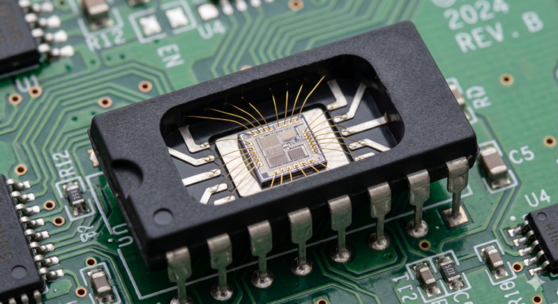
Imagine a microscopic city of billions of transistors – incredibly expensive, extraordinarily delicate, and so sensitive that a single speck of dust could destroy it.
For more than 50 years, Malaysia has been a global leader in encapsulating and connecting these chips through semiconductor packaging and testing.
We ship 13% of the world’s packaged chips this way.
The game today has fundamentally changed.
In the past, the process was simple: each package contained only one chip.
With the demands of AI, smartphones, AR/VR headsets, and other advanced applications, a single chip is no longer sufficient. It is no longer enough to meet the performance demands of today’s technologies.
The industry has moved toward “Chiplets.”
Chiplets can be arranged side by side, stacked on top of one another, and reconfigured like high-tech “LEGO” blocks to create a single, powerful superchip.
This means the process now begins with Integrated Circuit (IC) Design, but with a new twist. IC designers must now understand how these blocks will be stacked, interconnected, and arranged before they are even built.
If these chip architects do not understand how these “LEGOs” will be bonded together or tested later, the final product will simply not function.
Transforming a design into a finished product is now a sophisticated “LEGO” assembly process involving highly specialised equipment worth millions of dollars and precision beyond the capability of the human eye.
Imagine placing more than 10 microscopic solder connections across the width of a single human hair. That is the precision required to bond chiplets together. And then test to make sure the assembly works.
This needs a very complicated and interconnected chain of machines costing millions, with expertise and excellence in how to use them:
This process is now so complex and moves so fast that no single company can master it alone. Traditionally, local companies relied on multinational corporations (MNCs) to provide the designs and technical specifications. For traditional chips, we still do.
Malaysia became recognised globally for excellence in manufacturing execution. Made in Malaysia.
But to lead in the age of AI, we must move from following customer instructions to understanding “external trends” (anticipating global needs).
And charting our own course alongside our customers.
It is not an easy task and it is something Malaysia has not attempted before.
This is why we need a “Collaborative Mission” – a coordinated effort involving partners across every stage of the supply chain.
In support of this vision, Malaysia’s Advanced Packaging Consortium (MAPC) was formed by five local champions:
Together, these five companies form an industry consortium united by a common mission.
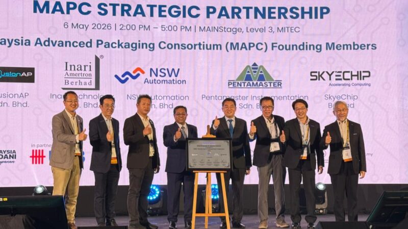
The mission of the MAPC is to build a complete, home-grown Advanced Packaging ecosystem from scratch. This shift – from “following instructions” to “defining the roadmap” – is a pivotal moment for our nation.
It is the intention of our National Semiconductor Strategy (NSS), announced in May 2024.
We are no longer just putting expensive chips in packages; we are attempting to design our future.
Standing still is not an option.
By working together, they have a greater opportunity to shape Malaysia’s future, contributing to tech development by solving problems before the global players even ask. To do that, they have to work with others, locally, regionally and globally.
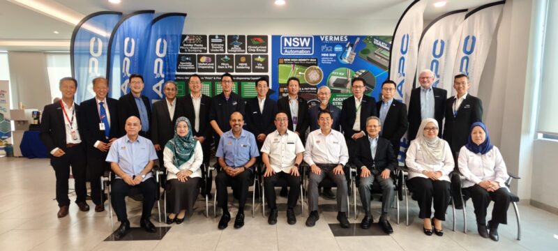
That is why three Government ministries – Ministry of Science, Technology and Innovation (MOSTI), Ministry of Investment, Trade and Industry (MITI) and Ministry of Economy (KE), recently visited Penang to better understand the progress being made to bring MAPC to life. They saw a future where Malaysia is not just a “high-tech” manufacturing hub, but an emerging global innovation hub.
They heard about the mission goal: “To enable the nation to capture 7% of worldwide advanced packaging shipments by 2035.” Today, Malaysia is just beginning that journey
In the world of AI, standing still is not an option. Neighbouring countries are moving quickly and building their own capabilities. They will not need 50 years to reach where Malaysia stands today.
Malaysia Boleh!
Explore other related content to further
explore MIDA’s insights.


